Characteristics of wastewater in the semiconductor industry
—— "High-risk wastewater under high-purity process"
The semiconductor manufacturing process is complex, involving multiple high-precision steps such as etching, cleaning, photolithography, CMP, ion implantation, etc. The wastewater produced has the remarkable characteristics of diverse pollutant components, highly refined content, and extremely high treatment standards:
There are more than ten types of wastewater: such as acid-base wastewater (pH 1-13), fluoride-containing wastewater, heavy metal wastewater (Cu, Ni, Cr, etc.), high COD organic wastewater (photoresist residue), high salt wastewater, high ammonia wastewater, etc., with different properties and cannot be mixed.
Fine ingredients and high toxicity: Some wastewater contains trace but highly toxic organic solvents, chelating agents, surfactants and heavy metals, even ppb (parts per billion) level residues may affect the quality of recycled water.
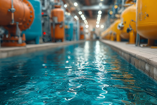
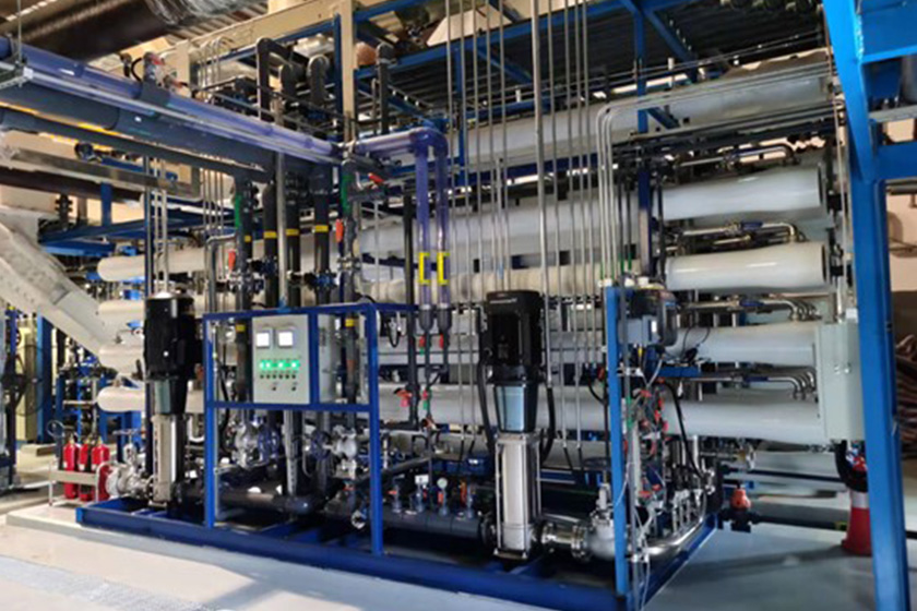
Ultra-high standards: In order to ensure the safety of production and clean room water quality, companies usually require that the quality of wastewater reuse water meet or even exceed the urban tap water standard, with total organic carbon (TOC) < 50ppb and conductivity < 1-2μS/cm. Ultrapure water standard treatment ideas must be adopted.
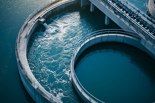
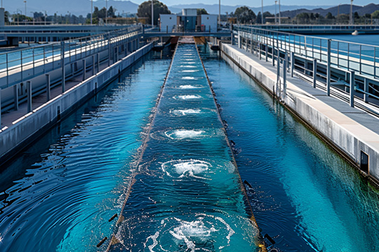
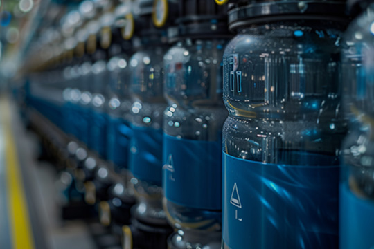
Huge water consumption, extremely high reuse value: A 12-inch wafer factory can consume 10,000-20,000 tons of water per day. If the wastewater reuse rate is increased by 1%, nearly one million tons of water can be saved each year, which is a key link in green manufacturing.
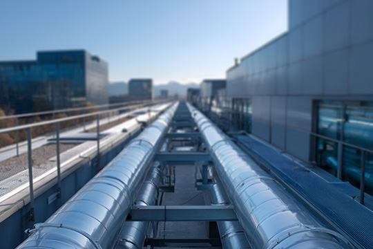
Extremely stable operation requirements: The semiconductor wastewater treatment system needs to operate continuously and stably 24 hours a day. Any fluctuation may affect the process operation and production line yield, and the fault tolerance space is extremely small.